THE SUPERTEF 96
The SUPERTEF, created end of 1998 was revised in 1990 and again in 1992. We are happy to present the fourth version of this RC transmitter: the 1996 model!
Aware of the difficulties facing the modelists, first in getting the electronic
supplies and second in their assembly, we have personnaly put significant
efforts on resolving those irritants to facilitate everybody's life.
The first SUPERTEF version was using a 68HC11 microprocessor in extended
mode i.e. with an external memory program which necessitated many integrated
circuits (IC) such as the 74C138, 74C373, 68HC24 and 27C64 making the printed
circuit board densely populated and prone to defects. Now, SUPERTEF 96 uses
a 68HC711E9 that is to say the same basic chip but with an INTERNAL program
memory operating in "mono-chip" mode without the need for all the IC's above.
The coder then became ultra-simple and except for monstrous errors, cannot
not function since all that is active is IN the microprocessor. The INTERNAL
storage in question has a capacity of 12 Kbytes instead of the 27C64's 8
Kbytes. The program is more performant. Let us say that it was necessary
all the same to add a small external memory storage to place the data for
27 possible models.
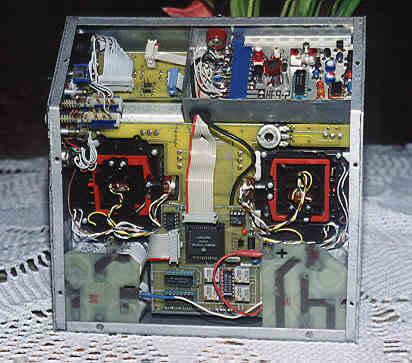
With regards to the assembly, the careful design and conception of the printed circuit boards made it possible to reduce the number of wires to be soldered considerably. However, experience has shown that soldering is difficult for non-professionals. Almost all the connections are therefore ensured by flat cables with crimped connectors. Only the stick controls are linked by ordinary wire because it is impossible to do otherwise. We can thus take apart the SUPERTEF WITHOUT USING A SOLDERING IRON! The picture showing the inside of the case is the ultimate proof!
Remained the problem of the case which you will not be able to buy off the shelf. There again, we tried to find a construction technique accessible to everyone. We believe that a modelist, worthy of this name is perfectly able to complete this work, which even if it is not very satisfying, is doubtless very profitable, strongly reducing the cost of the assembled SUPERTEF. Let us note that the author will be able to provide you with a decorative decal for the front face giving a professional look to your transmitter.
The software of the SUPERTEF 96 was also updated. All the possibilities of the previous versions are still there of course, but we added a total suppression of the jitter on the signal; an easier management of the main and safety frequency; model naming with eight alphanumeric caracters for each of the 27 models, divided into 3 groups of 9 memories, accessible by buttons for the second (Confbis) and third configurations (Confter); and finally an automatic programming of the models, which allows a high-speed "cleaning" of the whole memory... to mention only these 4 features!
THEORETICAL EXPLANATIONS
Figure 1 shows the diagram of the analog part of the coder. You see on the left the 4 amplifiers (U3) of the sticks' voltage (v1 to v4) with adjustment of the gains using P1 to P4 and the neutral fine adjustments, using P5 through P8. The outputs (0 to +5V) P0 to P2 are sent directly to the microprocessor. On the other hand, the auxilliaries (v5, v6 and v7), the trims (TR1 to TR4) and the gas channel (v4) are multiplexed by U1 and U2 in synchrony with the signal, before being transmitted to the microprocessor (PE3 to PE7). The circuit U3 should preferably be a LM660 from NS, with an output of 0 to +5V. Under these conditions, one can make VRL=0V and VRH=+5V, (they are the levels of reference of the A/D converter of the 68HC711) which is obtained with R12 = R13 =0. However the printed circuit makes it possible still to use a MC14573 with R12 = R13 = 47 ohms and the addition of R18. The amplifier U4A leads the tension of VARICAP of the frequency synthesized HF module and thus allows an alarm if the range of authorized variation is exceeded. The amplifier U4B formats the PPM signal by giving it the amplitude of 8V DC and the tilted sides necessary to obtain a correct HF spectrum figure. Fig. 2 illustrates the superb simplicity of the coder logic: U5 and... that is all! Port E is the 8-bit A/D converter of the microprocessor. Note that with 8 bits, it is possible to define 256 levels of precision. Knowing that a servo normally turns only 90 degrees, that gives us an accuracy of 90/256 = 0.3 degree approximately. So when we read in advertisements for instance that "... demanding pilots need an accuracy of 10 bits ….) that is to say 1024 levels, each one 0.08ø (yes, 8 hundredths of a degree!) we... laugh, quite simply! Port B manages the LCD display of 2x16 characters. Port C manages the keyboard and all the function switches. Port A has various missions: signal output, recognition of the type of HF module inserted, tachometer, buzzer.. Finally port D ensures the communication with the peripherals: model memories (U6), frequency synthesis HF module and an RS232 connection to another SUPERTEF or to a PC. The small circuit U7 ensures a correct reset of the microprocessor at power up, while the diode D18 protects all this small world from excessive voltage. Figure 3 represents all the connections ensured by the principal printed circuit board (referred as the T board because of its T-shape). This PCB collects the continuous voltage of the sticks, trims and auxilliaries. It hosts the dual-rate buttons DR1 to DR3, and those mixing CP1 to CP3 on channel 8. Lastly, the T board hosts the power circuits and the 5V and 10V regulators. Also, the T board conveys the signals PC0 to PC7 going to the keyboard, through connectors CONN3 to CONN6, but also necessary for all other functions of the board itself. Figure 4 is the diagram of the keyboard and appendices. One finds there the 4 keyboard input buttons, P, E - and +, the transistor commanding the buzzer, connectors CONN7 to CONN9 linking with the T board and the accessories located on the right side of the transmitter.
THE CONSTRUCTION
Very curiously, the SUPERTEF 96 although very complex in itself, is very easy to realize and can be assembled by any modelist, without any sophisticated measuring tools. A simple multimeter is enough if the person is careful and likes work well done! We replaced the special switches on older version 90 by ordinary ones easier to find. Moreover, their installation is done by a simple round hole of 6mm and these holes are hidden after assembly. The rectilinear potentiometer can be a model for SLM trim or a longer Radiohm.
1. THE CASE Below, interior of a finished SUPERTEF 96
a) CASE SIDES
Start by cutting out a template. See fig. 5A. Preferably out of 5mm aluminum failing this, out of beechwood. Measure and cut very carefully. Then cut out from some single sided epoxy plates 16/10, the right and left sides, copper inside, making sure you exceed the dimensions of the template by 1.5 mm approximately all around. Cut out of tinplate 5/10, some 8mm wide bands of lengths equal to those of each of the 6 sides of the template. Tin the copper of the sides. Install the template on the copper of one of the sides. Center carefully and keep in place using a soft clamp or something similar. Place one band at a time against the section of the template. Support well and tack for now with some light solder points only. After all bands are fixed, remove the template and solder by the interior until obtaining a beautiful joint all along the band while making sure it does not move, obviously. Sand the outside solder joints. Finally, consolidate the exterior angle with cyanolite glue. By using an aluminum band of 10/10 as a spacer, sand the external edges of the sides until being level with the aluminum. Drill holes as indicated on Fig. 5B and 5C. Chamfer the external edges of the sides.
b) FRONT FACE See Fig. 6.
It is preferable to use ordinary aluminium, easy to bend and not any unspecified alloy sometimes stiffer than steel. Cut the outside edges with a carpenter's or carpet knife: make several passes with a ruler. Make a deep groove. Fold down on a sharp, straight table edge and it will break clean. Also note that marking the line with a knife where you will later bend the faceplate produces a much better edge. Practice on an aluminum scrap piece. All inside holes are to be cut out using a metal saw. Bending requires two straight narrow pieces of hardwood which will hold the aluminum plate on each side, either with clamps, or with a vice. NEVER use a hammer directly. Bend by putting a straight piece of wood over the entire length. If you don't, the hammer will leave permanent marks. The distance between each bend are indicated "approximately" on the drawings. Once you have done the first bend, put the faceplat on top of the sides and mark the next location of the bend. These angles should be perfectly square with the side edges, or else the case will be twisted. Be careful, the top and bottom 8mm bands must be bended so that their external side matches the sides of the back tinplate bands exactly. This is so that the bottom rests correctly on all four sides of the case. If inside cuttings are made before folding which is recommended, begin bending with the angle between the future location of the LCD display and the sticks (145 degrees) then continue towards the end by putting the faceplate on top of the sides each time a bend is to be made to check your work. Now with the faceplate bent and cut, position the sides mark the location of the junction holes. Drill these holes in the tinplate bands and solder 2 mm brass nuts inside, these solder joints are easier made if the nuts are sanded (do not sold the top nut, on the side where the HF module will fit).
c) BOTTOM (not represented)
It is made out of a simple aluminum 10/10 plate, of 200 mm width and bent at an angle of 145 degrees. It will be assembled to the case by 3 bolts on the sides and 2 others on the bottom, ensuring at the same time the fixation of the two battery packs. These holes correspond exactly to their counterparts on the front face.
d) CASING OF THE HF MODULE See fig. 7A and fig. 7B
Prepare a rectangular template 115 X 65mm, out of 5 mm thick aluminum or beechwood. Cut out the form in tinplate of 5/10. Use the template to bend back the 3 sides, then the edges " a " and " c ", towards the inside, whereas the edge " b " is to be folded down towards the outside. The HF module casing should be located on the left side, as high and far back possible. Tack with 2 or 3 solder points. Check that it is square. Redo if necessary. Solder flap " b " onto the epoxy plate, then solder in the angle on the small accessible side. Normally the flaps " a " and " c " must be symmetrical in the window of the side, whereas " b " is sitting in the middle on the corresponding edge of the window. Thus the module closing plate, carefully cut out to the dimensions of the window, will take support on " a ", " b " and " c ". Raise the left side on the front face. The HF module must in theory, rest against the 8 mm aluminum edge. Mark the square hole of the antenna on the tinplate. Drill this hole, also drill that of the wire grommet, then drill the left higher hole of 2 mm. Solder on it a 2 mm nut. If you already have the printed circuit of the HF module, prepare the 10 X 10mm slides in beechwood and finally glue with Araldite. Finish by the installation of the HF module connector maintained by 2 bolts made out of 2 mm vertical pins going through the bottom of the case. It will be necessary to install a thickness of tinplate between the HF casing and the top face of the front faceplate, aligned with the square hole if one wants to preserve a perfect parallelism.
e) COMPLETION
Sand the surface of all faces finely, front, bottom and sides. Paint the whole case with a fuel resistant paint of the color of your choice. We prefer hammered gray, but that engages only us! The author will be able to provide you with a decorative decal in 2 parts, either in blue with white lettering, or aluminium with black lettering. It will be up to you to varnish it (using V33 for example). Before installation, mark with a small punch, the center of some of the essential holes. Remove the paper of protection and apply CAREFULLY. You are not entitled to make mistakes! Once installed, it cannot be moved! The punch marks are used as reference for installation, through the holes of the case. Press strongly, especially on the edges and the angles. Cut out the holes AFTER INSTALLATION, using a knife with pointed blade (blade nø 11 of Xacto)
1. PRINTED CIRCUIT BOARDS
There are 3: one (T board) supporting the commands and the coder, one circuit for the coder and another one for the keyboard. All 3 are double-faced with metallized holes. You should not try to make your own. The author will organize bulked orders, insofar as there are at least 10 requests. As for the remaining 4 identical circuits supporting the battery packs. They are single-faced, and very easy to realize. See Fig. 8.
2. LIST of ACTIVE COMPONENTS
U1, U2 4053
U3 LM660CN RS
U4 TDB0158DP ED ( or LM358 )
U5 MC68HC711E9CFN2
RS to be programmed by the
author
U6 27C16N RS
U7 MC33164P RS
U8 LM317
U9 7805
D1..D17 1N4148
D18 1N5908 ED
D19 1N4007
T BC547B
TO92
1 LCD display 2x16 character, type LTN211
3 PASSIVE COMPONENTS
CMS 1206 CMS 1206 except if indicated
R1 33 kohms; e/v1
C1 10 nF desc./v1
R2 33 kohms; e/v2
C2 10 nF desc./v2
R3 33 kohms; e/v3
C3 10 nF desc./v3
R4 33 kohms; e/v4
C4 10 nF desc./v4
R5 suppr
C5 10 nF desc./PE4
R6 33 kohms; pol+/U3
C6 10 nF desc./PE5
R7 33 kohms; pol-/U3
C7 10 nF desc./PE6
R8 1 Mohms; aj/v1
C8 10 nF desc./PE7
R9 1 Mohms; aj/V2
R10 1 Mohms; aj/v3
C10 0.1 uF VRH
R11 1 Mohms; aj/v4
C11 0.1 uF VRL
R12 0 ohms; VRL/TE
C12 4.7 uF pt16V +10V/U4
R13 0 ohms; VRH/TE
C13 4.7 uF pt16V pol/U4
R14 220 kohms; s/PA6
C14 4.7 uF pt16V +5/conn2
R15 33 kohms; pol+/U4
C15 0.1 uF mc/2.5 +5/conn2
R16 15 kohms; pol-/U4
C16 0.1 uF m C/5 D18
R17 1 Mohms; eVAR/U4
C17 4.7 uF pt16V 27C16
R18 3.9 kohms; if 4573
C18 10 nF desc./PE3
R19 12 kohms; PA0
C19 27 pF Qz
R20 12 kohms; PA1
C20 27 pF Qz
R21 12 kohms; PA2
C21 0.1 uF mc/5 +5
R22 12 kohms; ModA
C22 0.1 uF mc/5 +12V/HF
R23 12 kohms; ModB
C23 0.1 uF mc/5 ref/317
R24 10 Mohms; Qz
C24 0.1 uF mc/5 +10V
R25 4.7 kohms; Reset
C25 0.1 uF mc/5 +5/v6
R26 22 kohms; PD0
C26 0.1 uF mc/5 +5/v7
R27 22 kohms; PD1
C27 0.1 uF mc/5 +5/Clav
R28 22 kohms; PD2
C28 10 nF mc/2.5 con/HF
R29 22 kohms; PD3
C29 10 nF mc/2.5 con/HF
R30 22 kohms; PD4
C30 10 nF mc/2.5 con/HF
R31 22 kohms; PD5
C31 10 nF mc/2.5 con/HF
plain 1/4W
R32 220 ohms; ref+/317
R33 1.5 kohms; ref-/317
R34 6.8 kohms; PC0
R35 6.8 kohms; PC1
R36 6.8 kohms; PC2
R37 6.8 kohms; PC3
R38 22 kohms; PC6
R39 22 kohms; PC7
Adjustables multiturn pots 10x10
R40 15 kohms; Mes12V+ inline pins adjustments at the top
R41 4.7 kohms; Mes12V-
R42 220 ohms; V6+
P1 220 kohms; G/v1 V43 220 ohms; V6-
P2 220 kohms; G/v2 R44 2.7 kohms; V7+
P3 220 kohms; G/v3 R45 2.7 kohms; V7-
P4 220 kohms; G/v4 R46 6.8 kohms; T/Buz
P5 100 kohms; Aj/v2 R47 100 ohms; e/TX
P6 100 kohms; Aj/v2 R48 100 ohms; e/RX
P7 100 kohms; Aj/v3 R49 100 ohms; e/TACH
P8 100 kohms; Aj/v4 R50 22 kohms; m/TACH
P9 10 kohms; Aj/Bat
4 OTHERS
1 printed circuit board kit (author)
1 printed circuit board kit for holding the battery packs
2 2-way sticks SLM electrical trims ( LEXT ou SELECT )
1 special SLM switch ( SELECT )
1 antenna 1.25m/9mm + base ( SELECT )
1 linear potentiometer SLM trim type (LEXT )
1 pot 4 mm shaft type P160, 4.7 kohms; ( SELECT )
1 button for M6 re. 63.001 ( SELECT )
4 square buttons D6
8 miniature switches, 6mm body, 2 stable positions
2 miniature switches, 6mm body, 3 stable positions
1 keyboard ITT 2 keys - see text - ( parts from RS )
1 buzzer 6V type DM-03 ou KS3606
1 female chassis connector DIN 7pins/45degrees
1 quartz 8 MHz low profile HC49/S ( RS )
1 PLCC socket 52 pins
2 DIL tulip socket 2x4 pins
1 DIL tulip socket 2x7 pins
2 DIL tulip socket 2x8 pins
1 female bar AMPMODU 1 row of 24 pins gold-plated ( RS )
1 female bar AMPMODU 2 rows 2x5 pins gold-plated ( RS )
1 male bar AMPMODU 1 row 24 pins gold-plated ( RS )
1 male bar AMPMODU 2 rows to be cut ( RS )
2 female tulip connector 2 pins
6 connectors HE10 to be crimped
2 of 2x5 pins females
2 of 2x7 pins female
1 of 2x8 pins female
1 of 2x5 pins
to be soldered on the printed circuit board
Flat cable of 10 , 14 and 16 wires
Flex wire ref 47-I et 47-J from LEXTR.
1 epoxy plate single face 16/10 pour the case sides
Aluminium 10/10 for the case
Tinplate 5/10 for the HF module
20 screws and nuts of 2mm by 5mm
6 screws and nuts of 2mm by12mm
2 screws and nuts of 2mm by 20mm
Brass tubing for spacers
Decals
10 VARTA type RSH1.3 cells
1 tubular fuse 2A and a fuse holder
2 Fast-on thimbles MetF
1 connector 2x10 pins 3.96mm for HF 928 series ( RS )
1 grommet
1 little insulated wire 1 cond.
Notes
pt16V = tantalum perl 16V
mc/2.5 = multilayer step of 2.5
RS = RADIO-SPARES
LEXTR = LEXTRONIC
SELECT = SELECTRONIC
ED = ELECTRONIQUE-DIFFUSION
Contact the author if you are having difficulties finding supplies.
5. ASSEMBLY
a) T BOARD.
See fig. 9 and 10. The 9 tumbler switches on the top side will hold it in plce in the case and are soldered directly onto the PCB. We use ordinary models with thimbles, because special ones made for PCB's are smooth. However the thimbles are too big for the PCB holes. With a pair of adjustable pliers, crush the end of the thimbles until the tubes are crimped. It is very easy and... inserts. Slightly fold the two extreme thimbles towards the outside to fit into the PCB holes. Assemble the switches on the top side by adjusting the nuts so that the T once soldered is 16 mm from the case faceplate. Install the T and solder all switches. Install on the faceplate the M/A SLM switch. Solder 3 wires onto the thimbles of the switch, such as they will be opposite the 3 corresponding holes of the T... and put it back in the case. If all is well, the two pins for the charging jack will fit into their holes. Solder the 5 points of the SLM switch. Now solder the potentiometer M5 so that it is well centered in the slit. Prepare connectors CONN3 and CONN4. Connect the male and female pieces. Take out the T and place the female pieces on the T side and the males on the CODER side. Insert the coder into these pins. Keep the two printed circuits one against the other, and solder all the wires of the two connectors. Finish off the T circuit by installing a few more components. Be careful when positionning the regulators. Locate the hole for the potentiometer M6. Check that it will fit through front face. Solder the flat cable nø 3 if it is ready and the connector CONN6 on the components' side followed by the battery pack wires ending with female Fast-on thimbles.
b) The CODER Fig. 11 and 12
Increase the size of the access hole to the adjustment P9, just enough so that the screw of P8 can enter there. Begin with the installation of the CMS, on the component side, then install and solder all the elements of figure 11. Pay attention to the direction of the PLCC socket. The socket of U3, if it is a LM660, must be pushed down, making room above for the two holes for a 2x8 pin socket of a possible MC14573. (With this latter installed, resistance R18 must be soldered). Before installating the adjustable P1 with P8, preset them to half-way. The pins of CONN1 and CONN2 must be protruding on the component side of the board. Solder all the CMS on the copper-side following fig. 12. CONN3 and CONN4 are already soldered.
c) The KEYBOARD Fig. 13 and 14.
Solder the 4 keys by one leg only. Mount the keyboard on the front face on spacers of 9 mm. Check the position of the keys and their operation. Adjust their position if necessary. Take out the board and sold all remaining legs of the keys. Solder the two 2-pin tulip connectors which are on the copper side. Finish by installing all the other components, then by the 3 males connectors CONN7, 8 and 9, whose pins should also go on the copper side.
d) CONNECTIONS
Prepare the control sticks. If both axes are in the same direction, to disassemble one of them, and reassemble so as to have a Right stick and a Left one. It is also necessary to cut the plate supporting the trims, above of the two handles (if not, it is impossible to assemble the T). Finish by preadjusting all the potentiometers to have, in neutral, the cursors well centered (to check with the ohmmeter). Mount the T board and sticks on the front faceplate. Make the connections between the sticks and the T board using small gauge flex-wire. Of course, for the potentiometers of the AILERONS and DIRECTION which are " floating " it is necessary to make a good but supple connection by fastening the extremities. The other wires do not have to be flexible. Install the display, protected by a rhodoïd (a piece of plastic acetate), using spacers of 5 or 6 mm. Prepare the flat cable nø 2. This cable connects on CONN2 of the coder, goes under, then goes back up to the 145 degree bend of the front faceplate towards the display. Separate the wires as shown in figure 15 and are solder one by one onto the display. This should be done carefully. Make sure these wire will not prevent installation of the HF module, removed for the circumstance. Prepare the flat cable nø 1, according to indications' of figure 15, flat cable nø 3 being already welded. Connect CONN7 and CONN8. Prepare the HF module connector by presoldering the wires going to the chassis, the +12V connections and the 4 capacitors. Fix it permanently to HF module casing. Solder the wires going to the chassis AS SHORT AS POSSIBLE to the bottom of this casing. See Fig. 16. Lead the wires from left side to the front face. By protecting the wire passage by a grommet, introduce all 9 separate wires of cable nø 1 and solder them onto the ad hoc thimbles. The 12V is brought by an armoured wire of very small diameter coming from HF+ and HF of the T board. There we use a " home-made " connector. See Fig 7. In the HF module casing, solder the braid to the tinplate.
e) RIGHT SIDE
A word initially on the second (Confbis) and third configuration (Confter) switchkeys. They are INDEPENDENT keys. In their normal position, the configuration selected is the default first 9 models (memories I to Q). Pressing on the top button gives access to Confbis, the second group of 9 models (memories R to Z), while pressing on the lower button accesses Confter (memories @ to H) whether the top button is pressed or not. You may purchase these buttons from RADIO-SPARES, in three available kits: modules 2 reversers (réf 174-3821), chassis for 2 modules (réf 174-3865) and round or rectangular colored buttons. The assembly of these components is very simple. Fixing them to the side is made by two 20mm nuts with spacers. Now install the other components: Fn/Fs switches, stopwatch, buzzer and DIN connector. The flat cable nø 4 ensures the connection with the keyboard. From CONN9, it goes to the top, then the wires are separated and passing under the buzzer re-unite at the end. Note that the closed contacts give: Fs, CONFBIS, CONFTER and stopwatch. We securized the position of the wires using two insulated guards (read wire!) on the copper of the side. You may use the free button contacts as relay points.
5. BATTERIES Fig. 8
The VARTA RSH1.3 cells are welded between the epoxy plates. The block side - BATT has a tubular fuse in a holder. Put the two battery packs in the case, mark on the front face and on the bottom, the location where the holding screws will be (in the lower copper of the plates supports). Take out the packs, drill the holes and to solder nuts on the inside. Packs are thus held easily and solidly. The two packs are then wired in series using a fixed wire, but the + and - terminals are connected using male Fast-on thimbles, for possible demounting without desoldering. Check carefully that the two attaching bolts located in bottom of the sides are not likely to touch the cells, possibly causing a nasty short-circuit. It is advisable to cut them to the minimal length.
6. STARTUP
Take out the coder. Connect the batteries, move the switch to ON and replace the fuse by an ammeter. One must mesure a current of 23mA approximately. In addition, measure the existence of the +5V and the +10V (in fact 9.8v) on connector CONN4. Check the action of the sticks by measuring the voltage v1 with v4 on the same connector (1.9 to 3.1V), and those of the trims and the auxilliaries (0 to +5V). If all is correct continue, if not try to find the cause. Power off. Install the coder without any of the components that may be taken out. Power on and check the arrival of + 5V and + 10V. All is good... power off. Install all the active components IN THE RIGHT DIRECTION. Connect all the cables. The fateful moment at last!! Install a strap (jumper wire) between the two pins of the keyboard, marked " C16 " (They are both at the BOTTOM). The 68HC711E9 is supposed to be programmed, both EPROM and EEPROM, of course! Power on and watch the screen. At the initial startup, the 16 character blocks of the top line are darkened. Then, the automatic process of programming the 27C64 begins. The first line displays in French of course: ECRITURE de: X (X going from @ to Z) then... The second line displays: LECTURE de: X (X going from @ to Z) then displays at the end of the line a " [ " will indicate the endtask. If the symbol " [ " appears, all is correct. The 27C64 was written correctly then checked and declared good for the service. If the process stops on any cell, then there is an anomaly, quite improbable by the way! If all is well, continue. Power off. Remove the strap C16 and power on again. This time, it is the screen of service which appears with a blinking cursor on the right-hand side of the MODEL NAME which is for the moment the first one, that is to say " @ " and this name is noted "@@@@@@@@". Indeed the 27 model memories are indicated by a letter, goinf from "@", " A", " B", " C "... up to "Z " and all the names are initialized by defect with the same character, the cell " M" having for example the name " MMMMMMMM". Let the cursor blink during 10 seconds marked by the display of time, then the cursor disappears and the SUPERTEF is operational on the first model. Check the indication of the voltage. Bring the display to the exact value by adjusting P9, through the adjustment hole of the coder. Use a multimeter in comparison. Press on both " + " and " - " keys at the SAME time. The display will show you the menu in which you can scroll using " + " or " - ". Put the cursor on " ST ". Press on " P " You are then at the sticks calibration screen. By moving M1 to M4 one can see on the screen the corresponding value read by the A/D converter, value which must go from 0 to 255 (top high of the screen). Two adjustments are available for each one: P1 to P4 adjust the gains of the amplifiers and thus are used to regulate the throw, the 4 other P5 to P8 adjust the NEUTRAL. Fiddle with these adjustments until reading, in neutral the value " 128 " plus or minus1 or 2 and in addition by moving the sticks either way to their maximum, you should get a reading of "0" or "255". It is sometimes difficult not " to erase " a setting while trying to also adjust the other. Keep in mind that the LATERAL sticks' adjustments can favour a half-throw to the detriment of the other. Be careful with the gas stick which has a particular behavior: When the lever is in full-gas (all up) one must read " 0 " whatever the position of the trim. On the other hand if the stick is at full idle (all down), the display should show approximately " 64 " if the trim is in the up position and " 0 " if the trim is down. The trim should also show " 128 " if the two settings are in neutral. Indeed the SUPERTEF 96 integrates these modes of action by software which previously required a small additional plate.
Notes
1. We have just seen that the installation of the strap C16, BEFORE POWERING ON, will program the 27C64 by default, as many times as you want to, without forgetting that the operation erases any particular model program.
2. In the same way the strap " 711 " located above the first, allows the automatic writing by default of the internal EEPROM of the 68HC711. As this operation will be made initially by the author, at the time of the EPROM burning-in of the program of operation, you DO NOT HAVE to make this operation at the startup. On the other hand, if necessary, it will be possible for you to set the EEPROM to the default values, using the strap " 711 ".
3. NEVER place the straps in question DURING the operation of the SUPERTEF, there is a risk of deteriorating lines PC6 and PC7 of the 68HC711. They should be put, SUPERTEF in POWER OFF.
4. Do not place both straps AT SAME TIME.
5. The total consumption of the SUPERTEF 96, without an HF module installed is around 38 mA.
It is now up to you to get to know your new machine, but for that, refer to the instructions which will give you all the information on this subject. Of course, an HF module must be inserted to have a useable transmitter. It can be the HF9-2 single frequency or the HF10 at two simultaneous frequencies (Documentation available on request to the author). These two modules, which work perfectly, are obviously using frequency synthesis, a technique which we have used for more than 10 years and on which we have accumulated a significant practical experience and, we must say, is UNIQUE! There again, as opposed to what one could believe, their construction is very easy and never poses the least problem. On the other hand, we must say that certain measuring tools are necessary, but the author never refused to adjust a module that an amateur sent him!! Two HF modules exist either in 41, or in 72 MHz. The 41 MHz module can even cover the 40 MHz, on request. They emit in " SUPERTEF " FM shift (modulation) that is Sm=0, but one can also choose the other shift, that is to say Sm=1, which is appropriate for European versions of MULTIPLEX, FUTABA or other transmitters. Whatever the shift selected, the spectrum is always centered on the rated frequency selected plus or minus 5 kHz within the legal limits of the selected band. Let us note that the side switch Fn/Fs makes it possible to emit on either the main NORMAL or the SAFETY frequency which makes it possible to use the RX19 receiver with frequency synthesis and scanning, described in the nø 660 and the nø 661 of Modèles Réduits Avions (MRA) magazine. In this case, the PPM signal then contains a PCM code of identification ensuring that the RX19 will accept only the signals of the proper transmitter. These lines finish the construction file of the SUPERTEF 96. We hope that you have found here all the information necessary to your construction, but we remain, of course, at your disposal for any additional information.